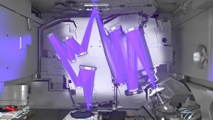
In advanced semiconductor lithography, the projection objective lens serves as the optical engine for high-precision pattern transfer. These lenses must deliver ultra-high resolution under extreme operating conditions, such as 193nm (ArF), 248nm (KrF), or 13.5nm (EUV) wavelengths. Assembly and alignment are critical stages, requiring rigorous control to achieve sub-wavelength tolerances.

I. Technical Challenges in Lithography Lens Assembly
At 02Optics, we have developed a closed-loop system that integrates precision assembly, active wavefront control, and full-environmental compensation. Here’s how we address core challenges:
1. Optical Axis Concentricity
- Maintain < 1μm decentering across lens groups
- Use 5-axis alignment platforms with coaxial CCD imaging
- Automated lens finding and incremental tilt adjustment per element
2. Tilt and Perpendicularity
- Keep tilt below 10 arcsec, flatness within 3μm
- Align lenses to housing base with < 5μm perpendicularity error
- Real-time angle verification using precision autocollimators
3. Wavefront Error (WFE)
- Measured by Zygo interferometers (λ=632.8nm)
- Achieve < 0.02λ RMS system-level wavefront performance
- Multi-wavelength testing & dual-path correction supported
4. Thermal & Refractive Stability
- Assembly room maintained at ±0.2°C, Class 1000 cleanroom
- Real-time air refractive index compensation
- Structural material selected for low CTE (Coefficient of Thermal Expansion)
II. Assembly Equipment & Environment at VYOptics
| Equipment | Capability | Purpose |
|---|---|---|
| Zygo Interferometer | λ/100 resolution | Wavefront and centering error measurement |
| 5-Axis Alignment Stage | 0.1μm linear, 2 arcsec angular | Precision tilt and decenter alignment |
| High-Precision Centering Lathe | <1μm shaping tolerance | Edge profile and optical axis alignment |
| Cleanroom & Thermal Control | Class 1000, ±0.2°C | Stable, clean working environment |
Our proprietary ALPS (Assembly & Lens Process System) platform logs every step in the alignment workflow, ensuring traceability and cross-batch consistency for mission-critical applications.
III. Application & Collaboration Models
We offer flexible engagement options for lithography OEMs and R&D teams:
- ✅ OEM / ODM full-lens assembly for EUV/DUV systems
- ✅ Large-diameter multi-element projection lens alignment
- ✅ Wavefront matching & hybrid simulation-measurement workflows
- ✅ Sub-nanometer centering with process data integration
Typical application scenarios:
- Semiconductor lithography projection systems
- UV mask aligners
- Sub-wavelength interference lithography
- High-NA EUV scanners
IV. Why Choose VYOptics?
As lithographic imaging systems move toward higher NA, shorter wavelengths, and tighter tolerances, precision optical alignment has evolved into a nano-engineering discipline. VYOptics combines technical rigor, advanced metrology, and integrated control systems to help our global clients achieve the next generation of lithography optics.
